当グループではLHD計測データ収集系(LABCOMシステム)の運転と、同実験関係者・共同研究者の計測データ収集・データ利用・遠隔実験等を支援する以下のサービスを行っています。詳細は各項目をクリックしてください。
English
You are the th visitor since 4 July 2000
Contact : LABCOM
プライバシーポリシー
各種フォームから個人情報を入力・送信する前に必ず上記をご覧ください。

8735 Timing Modulator


1.        General

8735 Timing Modulator is designed to generate patternized timing message associated with synchronized clock, prior to the trigger signal output (for example, 3 min, 30 sec, 10 sec, 0 sec before the trigger signal timing) initiated by a timing information signal.

This model has functions such as relay-transmitting and distributing timing signals from the higher level timing modulator.  Inhibit input such as emergency stop command, enables whole timing modulator actions disabled including delayed pulse output, and clock output.

This model also has a function to relay-transmit messages, which allows monitoring relay-transmitted message information.


2.        Hardware specifications

Reference trigger input

       Number of input                              8

       Input level                                       TTL pos logic pulse

Input connector                               CAMAC connector

       Input impedance                              10 kΩ

Inhibit input

       Number of input                              1

       Input signal                                     TTL neg logic pulse

       Input connector                               CAMAC connector

       Input impedance                              2 kΩ

External clock input

       Number of output                            1

       Output signal                                   TTL pos logic pulse

       Out put connector                            CAMAC connector

       Input impedance                              10 kΩ

Stop input

       Number of input                              1

       Input signal                                     TTL pos logic pulse

       Input connector                               CAMAC connector

       Input impedance                              10 kΩ

Setup input

       Numbers of input                             1

       Input signal                                     TTL pos logic pulse

       Input connector                               CAMAC connector

       Input impedance                             10 kΩ

Timing signal input

       Numbers of input                             1

       Input signal                                     Optical pulse signal

       Input connector                               FC connector

       Input baud rate                               20 M baud max

Timing signal output

       Numbers of output                           8

       Output signal                                   Optical pulse signal

       Output connector                             FC connector

       Output baud rate                             20 M baud max

LED display                                             Trigger input                     x 8

External clock input          x 1

Inhibit input                      x 1

Mode                                  x 2

Input enable setting          x 1

Relay-transmit setting       x 1

       Size

              VME standard 2 width module

       Power

              + 6 V, less than 1.5 A


3.        Software specification

3-1  Allowed setting address:   0xC0000 – 0xCFFFF

                                                 A7: By 2 bits dipswitches

                                                 A8 – A15: By 8 bits dipswitches

                                                  Possible base address, by these switches (BASE_ADD)

                                                                                           0xC0000

                                                                                           0xC0080

                                                                                           0xC0100

                                                                                           0xC0180

                                                                                                    -

                                                                                                    -

                                                                                                    -

                                                                                                    -

                                                                                                    -

                                                                                           0xCFF00

                                                                                           0xCFF80

                                                                                                          A1 – A6 are listed in a following table

As a function is pre-fixed (express as FIX_ADD), actual address (ADD) can be expressed as follows.

                                                        ADD = BASE_ADD + FIX_ A


Fixed address

Higher bytes

Lower bytes

Access

0x00

Not used

Control register

R/W

0x02

Not used

Mode register

R/W

0x04

Not used

Interrupt mask register

R/W

0x06

Not used

Trigger register

R/W

0x08

Not used

Interrupt register

R

0x0A

Not used

Event register

R/W

0x0C

Not used

1 sec timer trigger-selection register

R/W

0x0E

1 sec timer register

R/W

0x10

Transmitted message register (lower 16 bits)

R

0x12

Transmitted message register (higher 16 bits)

R

0x14

Not used

Manual-trigger execution register

W

0x16

Not used

Event execution register

W

0x18

Not used

Manual-inhibit execution register

W

0x1A

Not used

Manual-un-inhibit execution register

W

0x1C

Not used

Manual-setup execution register

W

0x1E

Not used

Manual-stop execution register

W

0x20

Not used

Phase-reset execution register

W


       3-2  Interrupt function

              Select one function from IRQ1 – IRQ7 by jumper connection

              Interrupt vector: Set by 8 bits dipswitch


       3-3 Interrupt factors:  Following factors generate interrupts.

              Trigger input:     When one of 8 trigger inputs activated, provided that input is enabled.

                                          During a relay-transmit mode, operable trigger message is one transmitted from the higher level modulator.

              Event input:        During a relay-transmit mode, when an event message is from the higher level modulator.

              Un-inhibit input: When inhibit is disabled (un-inhibit status).

                                          During a relay-transmit mode, when an un-inhibit message is from the higher level modulator.

              Inhibit input:       When inhibit is activated.

                                          During a relay transmit mode, when an inhibit message is from the higher level modulator.

              Error detection:   During a relay-transmit mode, when an error is detected in the higher level modulator.

              Clock input:         When no clock is detected or the clock-frequency is lower than the limit,             during external clock mode.

                                          During relay-transmit mode, when no reference clock is detected in the message transmitted from the higher level modulator.

Setup input:         When a setup-signal is activated, provided that input is enabled.

During a relay-transmit mode, when a setup message is from the higher level modulator.

Stop input:           When stop a signal is activated, provided that input is enabled.

                                                                       During a relay-transmit mode, when a stop message is from the higher level modulator.


4.        Register setting method

4-1  Control register (8bits)

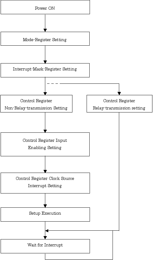
This is a basic register, therefore is to be set prior to start operation.

D0 sets the corresponded module to be used either as a relay-transmit mode “1” or as a master mode “0”.

D1 sets interrupt, enabled “1” or disabled ”0”

D2 sets a clock source, external “1” or internal “0”.

D3 sets signal input (trigger, stop, and setup), enabled “1” or disabled “0”.


Bit

D7

D6

D5

D4

D3

D2

D1

D0

Setting

***

***

***

***

1/0

1/0

1/0

1/0


       4-2 Mode register (8 bits)

              This is a basic register, therefore is to be set prior to start operation.

D0, D1, D2, and D3 correspond to Mode0, Mode1, Mode2, and Mode3, respectively.

One of the above bits is to be set “1”


Bit

D7

D6

D5

D4

D3

D2

D1

D0

Setting

***

***

***

***

1/0

1/0

1/0

1/0


4-3 Interrupt mask register (8 bits)

              This is a basic register, therefore is to be set prior to start operation.

Set interrupt-enabling-target-bit status to “0”. 

Initial status is all disabled “1”


Bit

D7

D6

D5

D4

D3

D2

D1

D0

Setting

***

***

***

***

1/0

1/0

1/0

1/0


                     “0” enable followings

                     D0: Trigger input interrupt

                     D1: Event input interrupts

                     D2: Un-inhibit input interrupt

                     D3: Inhibit input interrupt

                     D4: Error alarm interrupt

                     D5: Clock error interrupt

                     D6: Setup input interrupt

                     D7: Stop input interrupt


4-4 Trigger register (8 bits)

When a trigger input is issued by a message, interrupt will be generated (when enabled).

Readout of this register tells a channel number.  Writing an arbitrary number clears the register.


Bit

D7

D6

D5

D4

D3

D2

D1

D0

Setting

1/0

1/0

1/0

1/0

1/0

1/0

1/0

1/0


“1”: Under following conditions

                                             D0: When channel 1 is activated

                                             D1: When channel 2 is activated

                              D2: When channel 3 is activated

                              D3: When channel 4 is activated

                              D4: When channel 5 is activated

                              D5: When channel 6 is activated

                              D6: When channel 7 is activated

                              D7: When channel 8 is activated


       4-5 Interrupt register (8 bits)

              Readout of this register tells what is the element of interrupt

Readout clears the register, then interrupt will be terminated.


Bit

D7

D6

D5

D4

D3

D2

D1

D0

Setting

1/0

1/0

1/0

1/0

1/0

1/0

1/0

1/0


“1”: When interrupt generated

D0: Trigger-message-input interrupt

D1: Event-message-input interrupt

D2: Un-inhibit-message-input interrupt

D3: Inhibit-message-input interrupt

D4: Error-alarm interrupt

D5: Clock-error-alarm interrupt

D6: Setup-message-input interrupt

                         D7: Stop-message-input interrupt


       4-6  Event register (8 bits)

              Readout of this register tells what is the content of event message


Bit

D7

D6

D5

D4

D3

D2

D1

D0

Setting

1/0

1/0

1/0

1/0

1/0

1/0

1/0

1/0


       4-7   1 sec timer trigger selection register (8 bits)

              1 sec timer start-channel-setting register


Bit

D15

D14

D13

D12

D11

D10

D9

D8

Setting

1/0

1/0

1/0

1/0

1/0

1/0

1/0

1/0


                         “1”: When selected.

                         D0: Channel 1                                     D4: Channel 5

                         D1: Channel 2                                     D5: Channel 6

                         D2: Channel 3                                     D6: Channel 7

                         D3: Channel 4                                     D7: Channel 8


       4-8   1 sec timer register (16 bits)

              Elapsed time (starts when input activated to the trigger channel described above) in one sec unit.

              Writing an arbitrary number clears the register and stops elapsed timer counter


Bit

D15

D14

D13

D12

D11

D10

D9

D8

Setting

1/0

1/0

1/0

1/0

1/0

1/0

1/0

1/0


Bit

D7

D6

D5

D4

D3

D2

D1

D0

Setting

1/0

1/0

1/0

1/0

1/0

1/0

1/0

1/0


       4-9   Transmitted message register (32 bits)

              Transmitted 32 bits message can be readout.

              Lower word: D0 – D7 are synchronized codes (8 bits binary)

                         This code has the same value as 8 bits dipswitch’ set value

                         Transmitter modulator, receiver modulator, and relay-transmitter modulator use the same code setting.

                         D8 and D9 are 2 bits binary that represent modes as follows.

                                   Mode 0: 0b00

                                   Mode 1: 0b01

                                   Mode 2: 0b10

                                   Mode 3: 0b11

                         D10 – D15 are 6 bits binary that represent trigger channel (manual trigger as well).

                                   Channel 1: 0b000000                                     Channel 5: 0b000100

                                   Channel 2: 0b000001                                    Channel 6: 0b000101

                                   Channel 3: 0b000010                                     Channel 7: 0b000110

                                   Channel 4: 0b000011                                      Channel 8: 0b000111

                            Then, when transmitting un-inhibit:                                       0b010000

                            When transmitting inhibit:                                                      0b100000

                            When transmitting event-pattern, stop-message, setup-message, or phase-reset-message:

                                                                                                                              0b110000


Bit

D15

D14

D13

D12

D11

D10

D9

D8

Setting

TG 5

TG 4

TG 3

TG 2

TG 1

TG 0

M 1

M 0


Bit

D7

D6

D5

D4

D3

D2

D1

D0

Setting

ID 7

ID 6

ID 5

ID 4

ID 3

ID 2

ID 1

ID 0


              Higher word (D0 – D7) is event type (8 bits, bit pattern)

                            Followings are exceptional special codes

                            Stop message:               0b11110000

                            Setup message:              0b00001111

                            Phase reset message:     0b11111111

                            The trigger channel associated with these messages has the same pattern as the last time transmitted channel pattern.

                            D8 – D15: CRC-check-code (8 bits binary)


Bit

D15

D14

D13

D12

D11

D10

D9

D8

Setting

CR 7

CR 6

CR 5

CR 4

CR 3

CR 2

CR 1

CR 0


Bit

D7

D6

D5

D4

D3

D2

D1

D0

Setting

EV 7

EV 6

EV 5

EV 4

EV3

EV 2

EV 1

EV 0

       4-10 Manual-trigger execution register (8 bits)

                A trigger message can be transmitted by writing 8 bits trigger pattern (bit pattern).

                Execution starts when writing completed.  The message keeps the same contents as the message written to the channel, in which the trigger signal is routed.


Bit

D7

D6

D5

D4

D3

D2

D1

D0

Setting

1/0

1/0

1/0

1/0

1/0

1/0

1/0

1/0


                                 D0 represents Channel 1                            D4 represents Channel 5

                                 D1 represents Channel 2                            D5 represents Channel 6

                                 D2 represents Channel 3                            D6 represents Channel 7

                                 D3 represents Channel 4                            D7 represents Channel 8


       4-11 Event execution register (8 bits)

                An event message can be transmitted by writing 8 bits arbitrary pattern (refer to 4-9).

                The transmitting pattern is to be set to the event register described in 4-6.


Bit

D7

D6

D5

D4

D3

D2

D1

D0

Setting

***

***

***

***

***

***

***

***


       4-12 Manual-inhibit execution register (8 bits)

                A manual-inhibit message can be transmitted by writing 8 bits arbitrary pattern.

                This operation is same as receiving inhibit message.


Bit

D7

D6

D5

D4

D3

D2

D1

D0

Setting

***

***

***

***

***

***

***

***


       4-13 Manual-un-inhibit execution register (8 bits)

                A manual-un-inhibit message can be transmitted by writing 8 bits arbitrary pattern

                This operation is same as receiving un-inhibit message.


Bit

D7

D6

D5

D4

D3

D2

D1

D0

Setting

***

***

***

***

***

***

***

***


       4-14 Manual-setup execution register (8 bits)

                A manual-setup message can be transmitted by writing 8 bits arbitrary pattern.

                This operation is same as receiving setup message.


Bit

D7

D6

D5

D4

D3

D2

D1

D0

Setting

***

***

***

***

***

***

***

***


       4-15 Manual-stop execution register (8 bits)

                A manual-stop message can be transmitted by writing 8 bits arbitrary pattern.

                This operation is same as receiving stop message.


Bit

D7

D6

D5

D4

D3

D2

D1

D0

Setting

***

***

***

***

***

***

***

***


       4-16 Phase-reset execution register (8 bits)

                A phase-reset message can be transmitted by writing 8 bits arbitrary pattern


Bit

D7

D6

D5

D4

D3

D2

D1

D0

Setting

***

***

***

***

***

***

***

***


5.        Basic operation setting

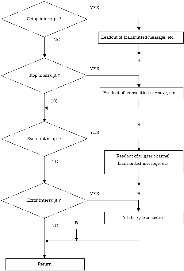
       Please set execution sequence, by setting-register, waiting-signal, and analyzing-interrupt-factors according to the following flow chart.